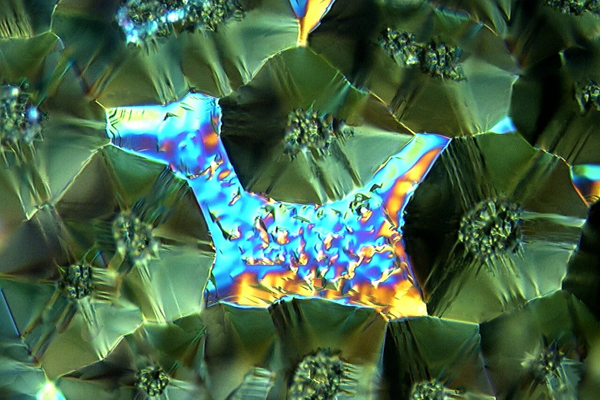
It is the sort of experiment that looks almost too simple to be real. Take two ultrathin crystal sheets, set one on top of the other, rotate it by a small angle, and then wait. According to a paper in Nature dated November 19, led by the Technical University of Denmark, the atoms at the seam rearrange themselves into a square grid, with no patterning tool touching the sample at all.
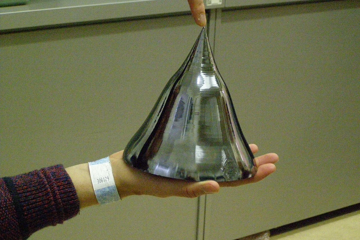
The material is strontium titanate, SrTiO3, and each sheet is roughly 10 nanometers thick. It was chosen precisely because it is unremarkable: hard, chemically stable, and a workhorse model oxide that electronics researchers have leaned on for decades. Unlike many delicate two-dimensional materials, it survives being stacked onto a chip, which makes it a practical candidate rather than a laboratory curiosity.
The first layer is the familiar one: ordinary moire.
Lay two mesh screens across each other and give one a slight turn, and a larger repeating pattern seems to float above them. Two regularly ordered crystals overlapping at a small angle produce much the same thing. Under a microscope, that is usually all researchers have been looking at: a geometric shadow, pretty, but not a physical structure.
This time the interface does more than cast a shadow. Strong bonding forces the atoms on both sides to shift and accommodate each other, and the leftover mismatch has nowhere to go, so it is squeezed into narrow lines of strained crystal. Those lines are dislocations, and here they link end to end into a square network.
That distinction matters. The grid is not a visual trick produced by overlapping lattices; it is the structure left behind after atoms physically moved. Confusing pattern with matter is the easiest way to read this paper too shallowly, and it is a mistake worth naming explicitly.
What makes the result interesting is the order: prediction came before the picture.
The atomic rearrangement was first anticipated in simulation, yet the early micrographs showed only ordinary moire, with no sign of the grid. The team turned to machine-learning models that compute how atoms move when thin layers bond and twist, and those models predicted what the square network should look like and where to hunt for it.
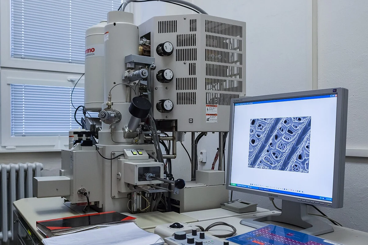
Only then did the experiment catch up. By simulating how an electron beam travels through the material, and by cutting the sample along several directions to inspect cross-sections, the researchers at the University of Antwerp in Belgium and the SuperSTEM facility in the UK produced microscopy that lined up closely with the theory.
That methodology deserves its own line. This was not see-it-then-explain-it; a model narrowed the search space first, and the electron microscope was sent in to confirm. In materials discovery, that ordering is quietly shifting from exception to routine, and it is arguably the transferable result here.
The third layer is the one with electrical consequences.
The models also predict something more valuable than the grid itself. Around each dislocation, the strain nudges positive and negative charge slightly apart, creating local polarization that settles into vortex-like patterns. Polarization is precisely the knob that data storage and energy storage keep trying to turn, so these nanoscale vortices are not merely decorative. They could, in principle, be writable cells.
And the twist angle sets the spacing between dislocations, which is to say it sets the size of the grid. One team member put it plainly: the structural dimensions are tunable by rotation. For memory technology, controllable cell pitch is close to the starting point of every engineering ambition, because it suggests density need not only be etched downward. It might be dialed in by a twist.
Before anyone draws a roadmap, two questions are still hanging.
Do the grid lines actually conduct? Can the electrical patterns inside the cells be written and erased repeatedly, cycle after cycle? Until both are answered, there is no serious claim of reaching a practical threshold. The team's own next step is worded carefully: explore whether strontium titanate or other oxides can yield useful electrical behavior. That restraint is a signal in itself.
Step back, and the context is clear. Today's memory roadmap is dominated by lithography, pushing features smaller at ever tighter equipment and cost pressure, while self-assembly has long been promised as a way to let materials build themselves and has just as long been dogged by structures that refuse to behave. This work at least demonstrates that twist angle can serve as a continuous, predictable dial. But the deeper shift may be one of attitude rather than devices. Dislocations and grain boundaries have spent decades being treated as defects to eliminate; here they are recruited as a design variable that can be tuned continuously. From tolerating defects to conscripting them, materials science has quietly changed its mind about what counts as useful.



Comments